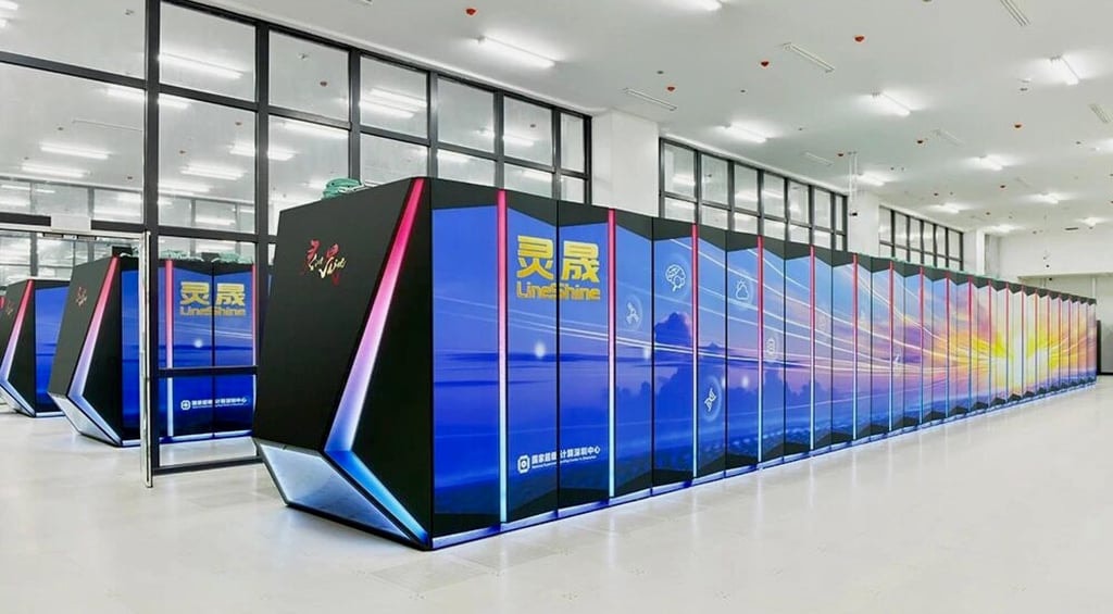
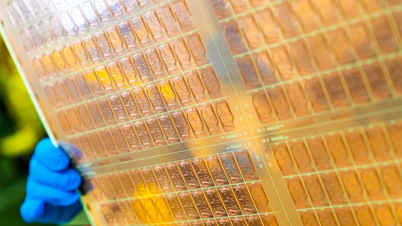
The transition from organic substrates to glass panel-level packaging (PLP) represents one of the most profound changes in semiconductor architecture since the advent of multi-core processing. Unlike incremental upgrades, this shift demands a complete reimagining of how chips are designed, manufactured, and delivered. Intel's recent $650 million investment underscores the urgency, but the path forward is fraught with technical and logistical challenges.
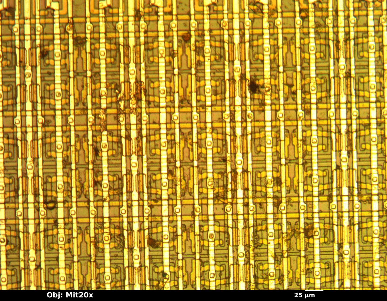
Glass isn't just a material—it's a platform for reinvention. Unlike organic substrates, which have long been the industry standard due to their flexibility and cost-effectiveness, glass offers superior thermal conductivity, electrical performance, and scalability. This could address critical bottlenecks in modern chip design, where heat dissipation and signal integrity are increasingly constrained by traditional packaging methods. The potential benefits extend beyond raw performance; streamlined manufacturing processes could significantly reduce production costs and accelerate time-to-market for next-generation chips.
The competitive edge
Intel's investment is a strategic move that aligns with its broader push to vertical integration, reducing dependency on external foundries like TSMC. While TSMC has been quietly advancing its own glass-based solutions, Intel's deep pockets and integrated supply chain could give it a decisive advantage in this race. However, TSMC's established leadership in advanced node production means neither company will dominate without collaboration or innovation from smaller players.
Market momentum and industry impact
The market for glass-based packaging is projected to surge from $650 million today to over $8 billion by 2030, but the transition won't be smooth. Material sourcing, manufacturing infrastructure, and design compatibility remain significant obstacles. For PC builders and OEMs, this shift could lead to longer product cycles in the near term as companies adapt, but long-term gains in efficiency and performance are expected to outweigh the challenges.
A new era for chipmaking
This isn't just another upgrade—it's a fundamental redefinition of semiconductor architecture. The implications ripple through the entire industry: supply chains will need to evolve, development timelines will shift, and product roadmaps will be redrawn. For now, the exact timeline remains uncertain, but one thing is clear: those who master glass-based packaging will set the pace for the next decade of computing.