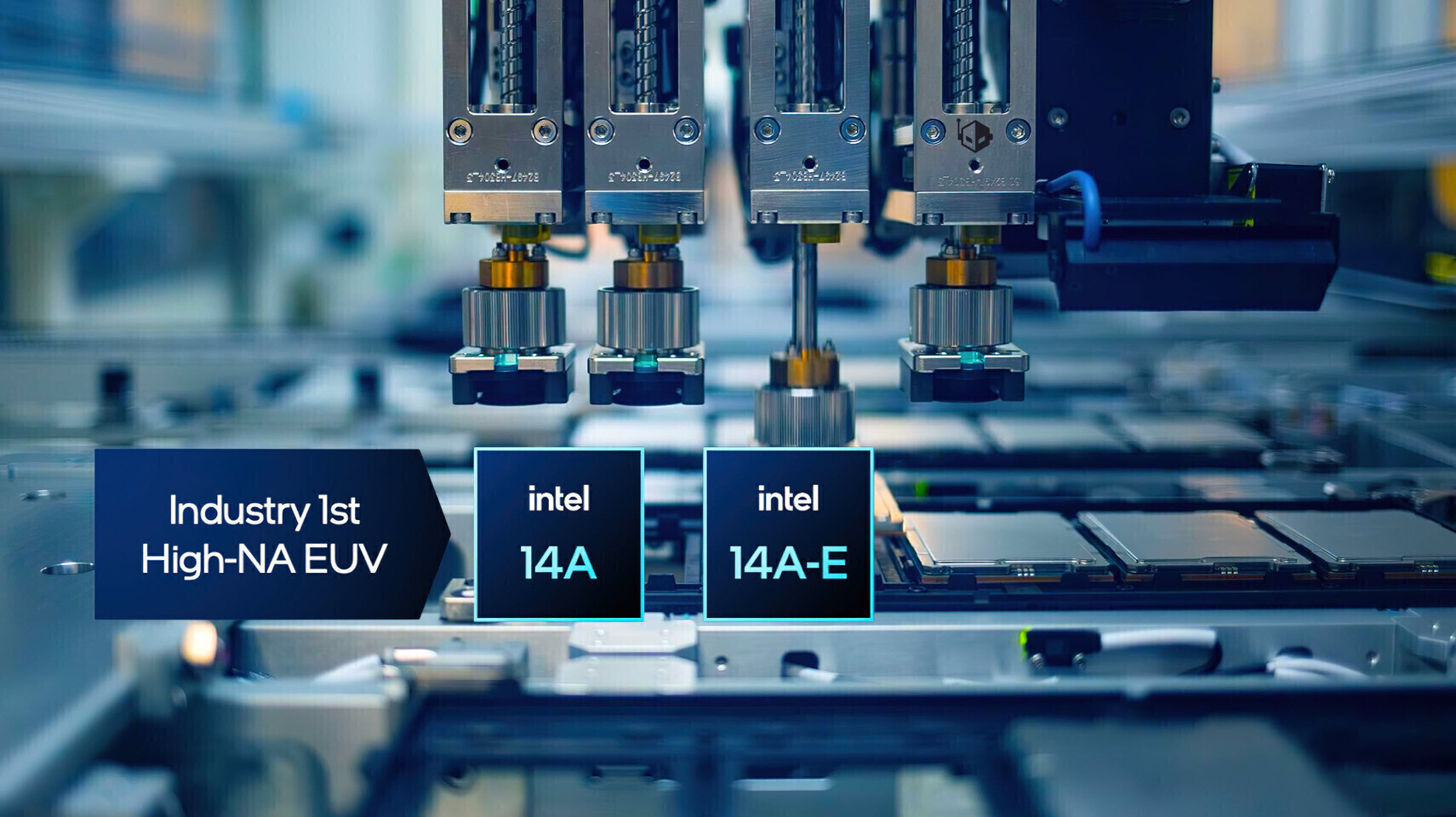
Intel's TeraFab project represents a major step forward in semiconductor manufacturing, promising to enhance production efficiency while cutting costs. The initiative, slated for full disclosure soon, could redefine how chips are made, offering power users and enthusiasts new possibilities.
The TeraFab facility is designed to leverage advanced packaging techniques, including Intel's Foveros technology, to combine multiple chiplets into a single, highly efficient package. This approach not only improves performance but also reduces the overall footprint of computing systems, making it an attractive option for high-performance applications such as AI and data centers.
Key to this project is its focus on scalability and cost reduction. By integrating advanced manufacturing processes, Intel aims to streamline production while maintaining high yields. This could lead to more affordable and powerful hardware for consumers and businesses alike.
The Impact on Power Users
For power users, the TeraFab project opens up new avenues for innovation. The ability to combine multiple chiplets into a single package allows for greater flexibility in designing high-performance systems. This is particularly beneficial for applications that demand both processing power and energy efficiency, such as AI workloads.

- Advanced packaging techniques enable more efficient heat dissipation and power management.
- Reduced footprint means smaller, more compact designs without compromising performance.
- Scalability ensures that the technology can be adapted to various use cases, from edge devices to large-scale data centers.
The project also addresses supply chain challenges by optimizing manufacturing processes. This could lead to shorter lead times and a more stable supply of high-performance components, which is crucial for industries reliant on cutting-edge hardware.
Everyday Users: What's in It For Them?
While the primary benefits may be targeted at power users and industrial applications, everyday consumers could also see indirect advantages. The cost reductions achieved through TeraFab could trickle down to more affordable hardware, making advanced computing capabilities accessible to a broader audience.
The focus on energy efficiency is another area where everyday users stand to gain. As devices become more power-efficient, they will require less energy to operate, leading to lower electricity bills and a reduced environmental footprint. This aligns with the growing demand for sustainable technology solutions.
Looking ahead, Intel's TeraFab project signals a significant shift in the chipmaking industry. By pushing the boundaries of what is possible in semiconductor manufacturing, Intel is positioning itself at the forefront of innovation. The full details of this initiative are expected to shed more light on its potential impact, but one thing is clear: this is a step that could redefine how we think about computing power and efficiency.