Intel Foundry is making a bold play for dominance in the semiconductor foundry market, leveraging its 14A node and advanced packaging technologies to compete with TSMC. The move comes at a critical juncture, as companies like NVIDIA, AMD, Google, and Apple evaluate alternatives to TSMC’s long-standing leadership.
The 14A node, combined with Intel’s EMIB and Foveros packaging solutions, offers a compelling alternative for high-performance designs. While TSMC has been the go-to partner for cutting-edge silicon, including NVIDIA’s RTX 5090 GPU—rumored to feature RDNA and Zen architectures at 2nm and 3nm nodes—Intel is betting that its advanced packaging can overcome historical reliability concerns.
Key features of Intel Foundry’s approach include
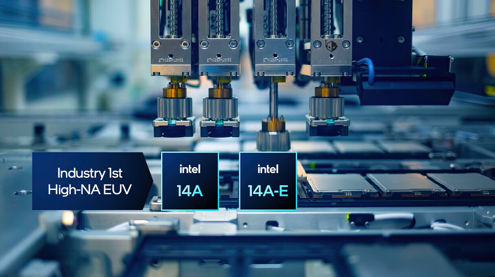
- 14A Node: A new process node designed for high-density, low-power silicon with plans to expand into 18A variants
- Advanced Packaging: EMIB and Foveros technologies enabling complex chiplet designs, including multi-kilowatt solutions for GPUs and AI accelerators
- High-End Support: Potential production of NVIDIA’s RTX 5090 GPU, which is expected to use a mix of RDNA and Zen architectures at 2nm and 3nm nodes
The challenge for Intel Foundry will be proving its reliability on par with TSMC, particularly for high-end products where yield and performance are critical. While TSMC has faced hurdles with larger dies—such as those used in NVIDIA’s RTX 5090 GPU—Intel’s EMIB technology offers a path to high-density, multi-chiplet designs without the same limitations.
For OEMs and power users, this shift could introduce new options for silicon sourcing, but it also brings uncertainty about performance consistency. If Intel succeeds, it could mark the first major disruption in foundry dynamics since TSMC solidified its dominance with 3nm and 2nm processes. The race is on, but the true test will be whether Intel can deliver the same level of maturity at scale.