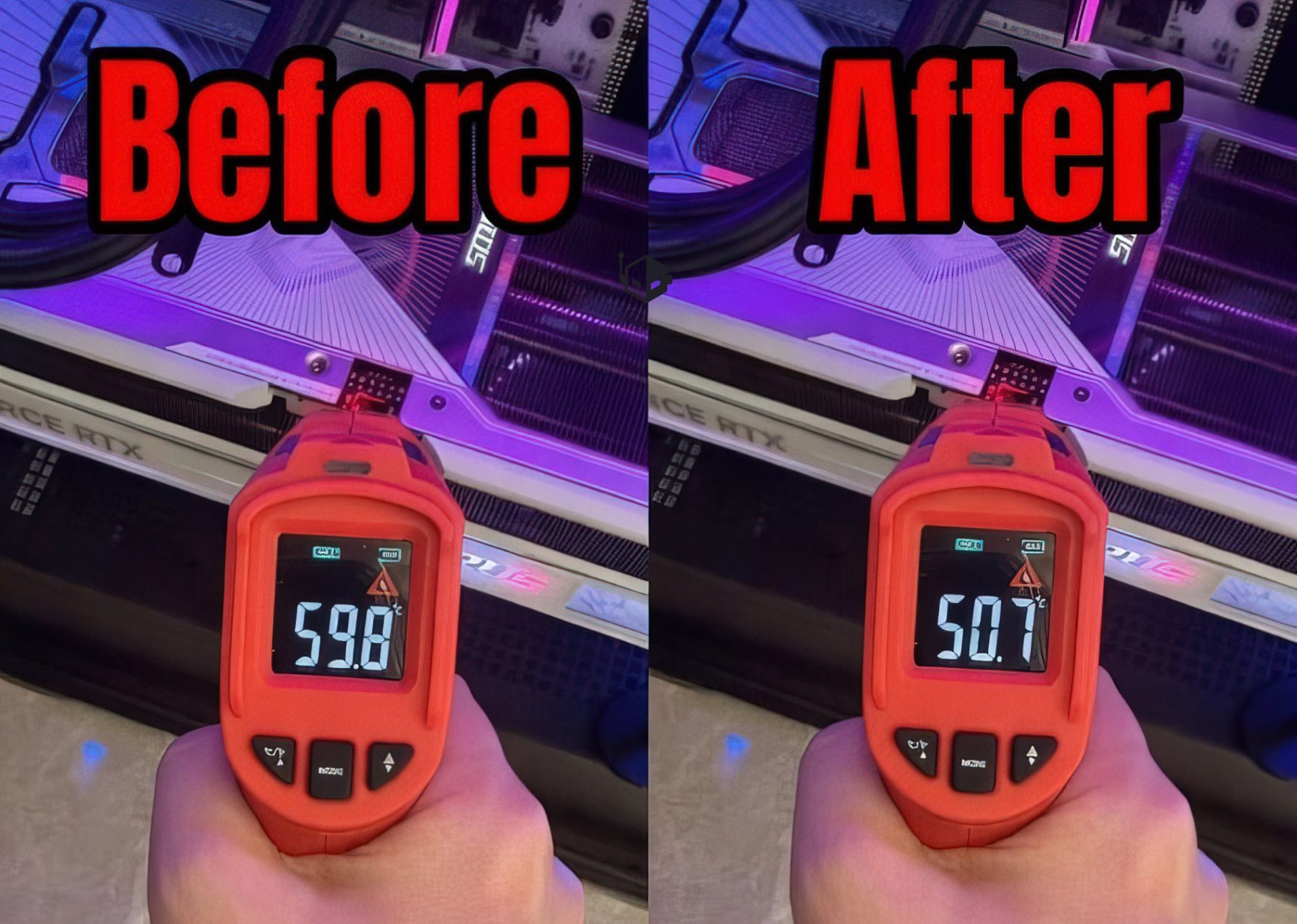
When Nvidia introduced its Blackwell architecture earlier this year, it wasn’t just another incremental upgrade. The shift from Hopper to Blackwell marked a deliberate pivot toward energy efficiency—a factor that could reshape how AI workloads are deployed in data centers.
The Blackwell platform, built around the GB200 Grace GPU, delivers up to 40 TFLOPS of FP8 performance while consuming significantly less power than its predecessors. This isn’t just about raw compute; it’s about doing more with less, a critical consideration as AI models grow in complexity and data centers face mounting energy costs.
At a glance
- Performance: 40 TFLOPS FP8, 256-bit memory bus, 128GB HBM3e
- Efficiency: Optimized for AI workloads with lower power consumption than Hopper
- Thermal Design: 270W TDP, liquid-cooled packaging
- Use Case: Targeted at large-scale AI training and inference tasks
The Blackwell architecture introduces several firsts. The GB200 Grace GPU is paired with a new system-on-chip design that integrates CPU and GPU cores on a single package, reducing latency between components. This tight integration is designed to improve performance in high-bandwidth scenarios like large language model training.

However, the transition isn’t without challenges. While Nvidia claims Blackwell is the most energy-efficient architecture in the world, industry benchmarks are still pending. Early adopters will need to weigh the promises of efficiency against proven alternatives—like Nvidia’s own Hopper or AMD’s Instinct MI300X—before committing to large-scale deployments.
For data center operators, Blackwell could offer a compelling path forward if it delivers on its efficiency claims. But with AI workloads evolving rapidly, the question remains: will this architecture stand the test of time, or will newer designs render it obsolete before it even hits the market?