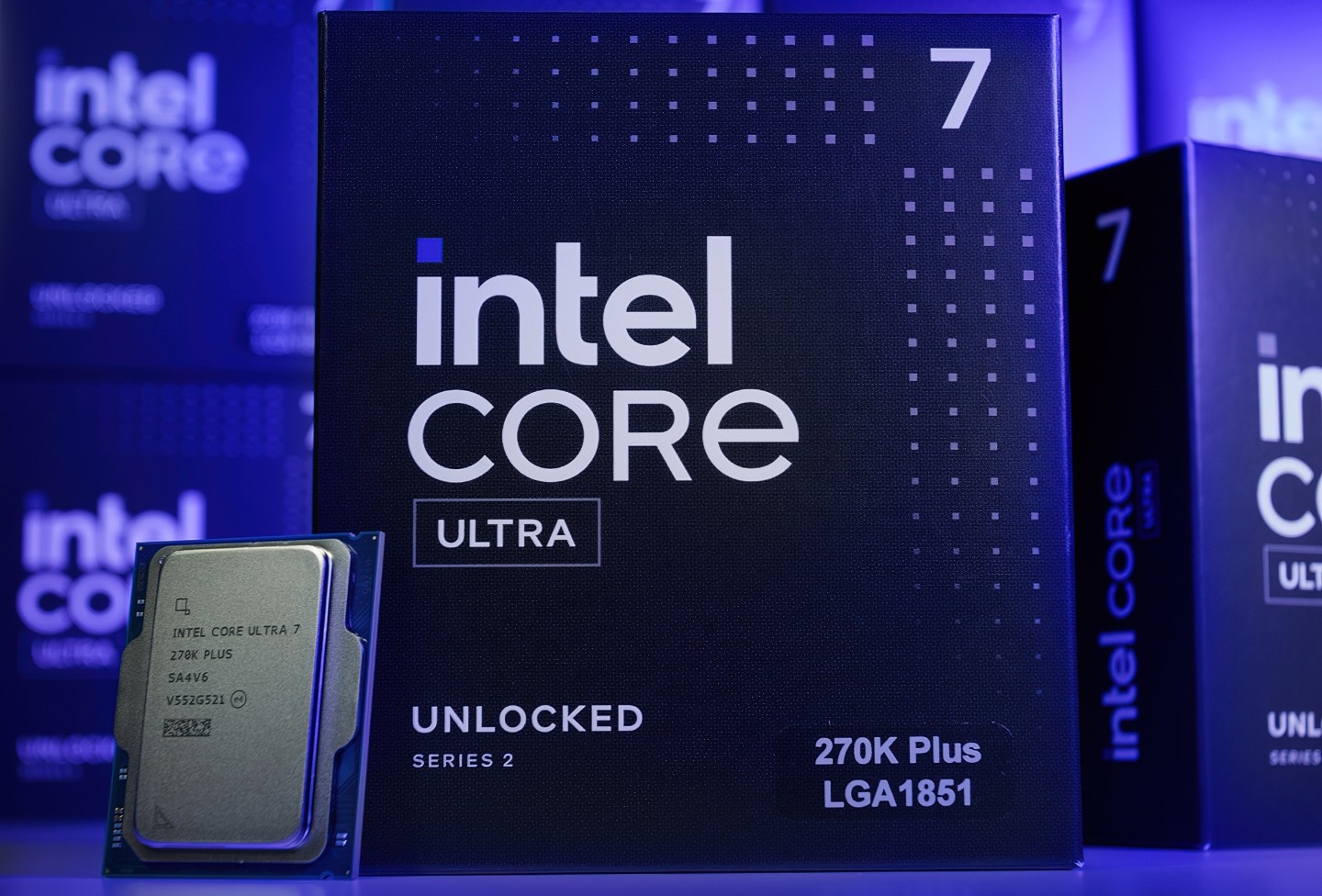
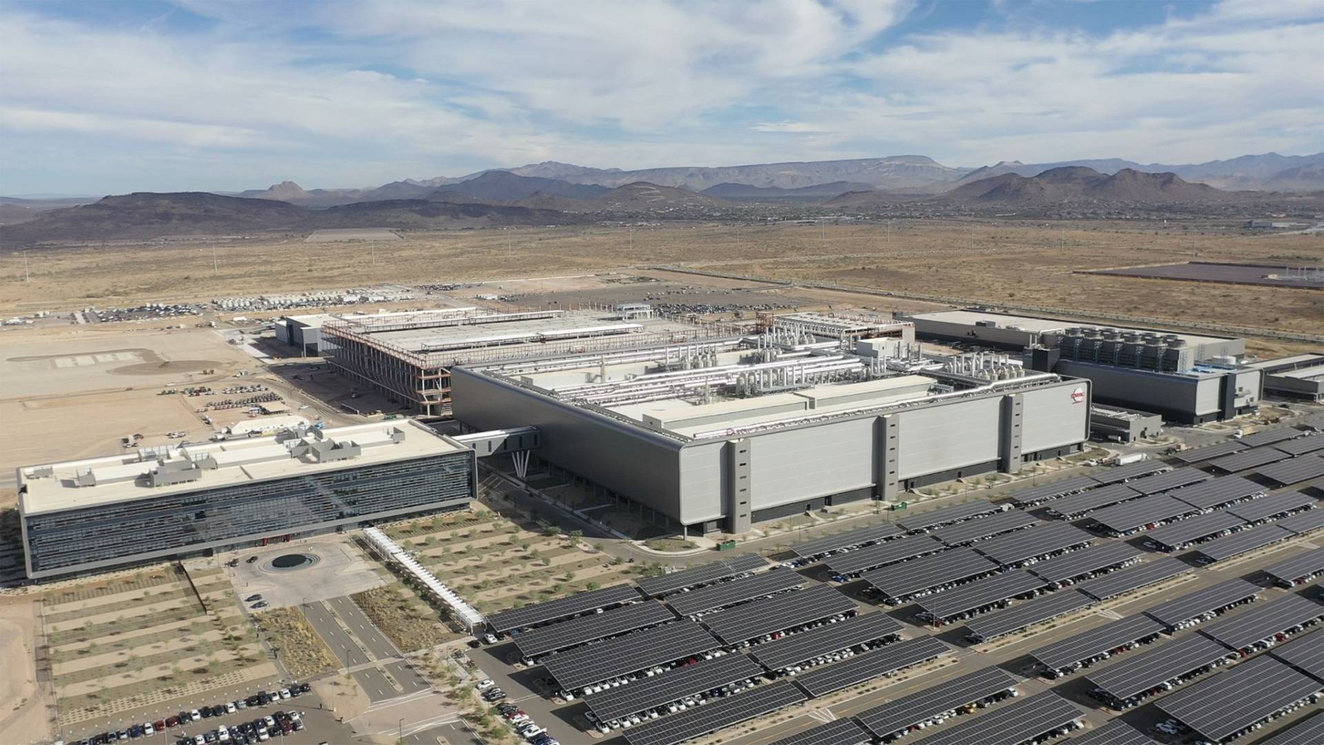
TSMC’s latest push into ultra-advanced semiconductor nodes is setting a new benchmark in chip manufacturing, but the path to 1nm production is fraught with uncertainty.
The foundry giant has begun outlining its roadmap for sub-2nm processes, aiming to bring 1.4nm to high-volume production by 2025 and start planning for 1nm as early as next year. This aggressive timeline contrasts sharply with Samsung’s decision to pause development on its own 1.4nm process, leaving TSMC as the sole leader in this ultra-fine manufacturing space.
At the heart of TSMC’s strategy is a focus on performance and efficiency gains that could redefine what’s possible in computing. The shift to 1.4nm is expected to deliver around 25-30% improvements in power efficiency over its current 3nm node, while also enabling higher transistor density. But the jump to 1nm—if it ever arrives—would require breakthroughs in materials and lithography that are still years away from practical implementation.
Performance vs. Reality
The implications for developers and hardware designers are significant. A 1.4nm process could unlock new levels of performance per watt, making it a critical enabler for AI accelerators, mobile chips, and high-performance computing. However, the transition to such fine nodes introduces complex challenges in yield, reliability, and manufacturing consistency.
Samsung’s decision to pull back from 1.4nm development signals a reality check in the semiconductor industry: not every node is viable at this stage of technological advancement. TSMC’s ability to push forward will hinge on its R&D investments, partnerships with equipment suppliers, and the willingness of chipmakers to adopt these cutting-edge processes.
The race to 1nm is less about immediate gains and more about securing a long-term advantage in semiconductor leadership. For now, TSMC holds the upper hand, but whether it can sustain this momentum remains an open question.