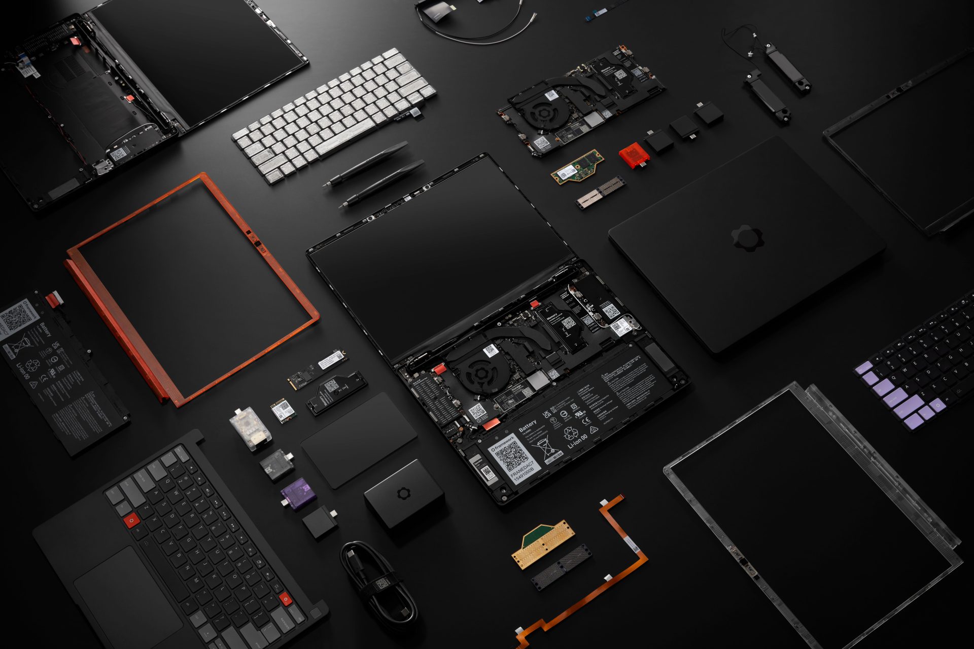
For the engineers building next-generation AI accelerators, high-bandwidth memory has always been a double-edged sword: it delivers the throughput needed for massive data flows, yet its physical constraints—thinner wires, tighter spacing, higher currents—push performance to the brink of failure.
Samsung’s latest move on HBM4E memory is an attempt to flip that script. By breaking up the power network into smaller, decentralized blocks and slashing metal-circuit defects by 97 %, the company has created a new baseline for reliability in stacked DRAM. At the same time, it’s testing whether the future of AI chips lies not in cramming GPU and memory closer together, but in separating them entirely—using photonic interconnects that can transmit terabits per second across distances once thought impossible.
This isn’t just an upgrade; it’s a rethink of how power moves through a chip. The traditional ‘honeycomb’ layout on the base die, used since HBM4, has been replaced by four smaller power blocks, each further subdivided in upper layers to reduce congestion and shorten routing paths. The result is less voltage drop across circuits—an improvement of 41 %—which means more headroom for clock speeds without sacrificing stability.

- Power Network: Segmented into four smaller base blocks, each further subdivided in upper layers to cut congestion and IR drop by 41 %. Metal-circuit defects reduced by 97 % compared to HBM4.
- HBM4E Specifications: 14,457 power bumps (vs. 13,682 in HBM4), thinner, denser wiring, headroom up to 13 Gbps per stack.
- Thermal & Photonic Exploration: Early tests suggest substrate wiring advances could allow HBM and GPU separation beyond 5 cm; photonic interconnects under evaluation for terabit-per-second links.
A user working with AI workloads would notice the difference in two ways. First, at the bench: fewer silent data errors during prolonged training runs, and a smoother power curve that lets clock speeds climb without sudden voltage collapse. Second, under the hood: the physical layout now allows for more parallel power paths, which can translate into lower latency spikes when multiple cores fire simultaneously.
But the bigger implication may lie in Samsung’s willingness to question the ‘stack everything together’ paradigm. If photonic interconnects prove viable at scale, the next generation of AI chips could see GPU and memory physically divorced—no longer bound by copper limitations or thermal hotspots. That shift would force a reconfiguration not just of silicon, but of how we think about data movement: from on-chip wires to light-based pipelines that bypass traditional constraints entirely.
The immediate takeaway is clear: HBM4E is no longer an exercise in cramming more into less space. It’s becoming a platform for experimentation—where power delivery, thermal design, and even the fundamental coupling of GPU and memory are open to reinvention. That flexibility could redefine what’s possible in AI hardware long before the next node shrink arrives.