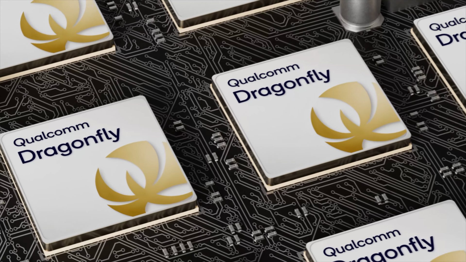
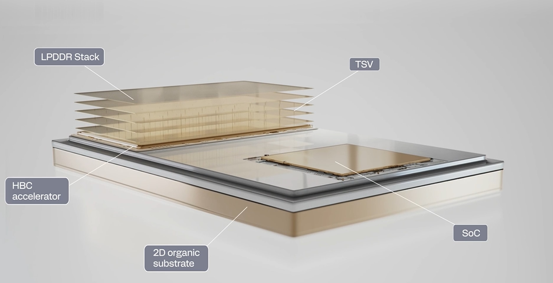
Qualcomm's High Bandwidth Compute (HBC) Gen 1 is poised to disrupt the landscape of memory and compute integration. Unlike conventional architectures that rely on horizontal memory layouts, HBC Gen 1 employs a vertical stack of LPDDR chips directly above a compute die, leveraging through-silicon vias (TSVs) to achieve unprecedented bandwidth efficiency. This design eliminates traditional bottlenecks, offering a performance leap that could redefine AI workloads and high-resolution graphics processing.
The architecture's most compelling feature is its ability to perform computations closer to the data source. In current systems, latency between memory and processor can hinder real-time applications like AI training or 4K rendering. By reducing this gap, HBC Gen 1 promises smoother performance in demanding workloads, potentially unlocking advancements in both gaming and artificial intelligence.
Performance: A New Standard for Efficiency
- Bandwidth: 133 TB/s—significantly surpassing LPDDR5X (typically around 7 GB/s) and DDR5, setting a new benchmark for high-performance computing.
- Efficiency: 6 times better bandwidth per watt than HBM4, leading to cooler operation and extended battery life for AI-driven devices.
The architecture's optimization for near-memory computation is a game-changer. Qualcomm's internal benchmarks suggest an 18x improvement over its existing AI200 card, which relies on standard LPDDR5X. This could translate to faster image recognition, more fluid ray-traced graphics, and breakthroughs in AI model training—all while maintaining power efficiency that traditional DDR-based systems struggle to match.
Challenges and the Path Forward
The journey to widespread adoption is not without its challenges. Manufacturing precision is a critical hurdle; stacking multiple layers of memory requires expertise that only a few semiconductor foundries currently possess. While Qualcomm has not confirmed partnerships, industry speculation suggests potential collaborations with leading foundries like Samsung Foundry or TSMC. If these partnerships materialize, HBC Gen 1 could see accelerated adoption, but delays would risk giving ground to competitors such as AMD, which is advancing its RDNA 4 architecture for AI-driven graphics.
Looking ahead, Qualcomm has hinted at the development of HBC Gen 2, promising even greater bandwidth. However, the first wave of devices is not expected until mid-2027, with the AI250 accelerator leading the charge. The question remains: Can Qualcomm deliver on this promise without encountering manufacturing bottlenecks? If successful, HBC Gen 1 could redefine how AI and high-performance computing share data—without sacrificing efficiency.
Implications for Gamers and AI Developers
For gamers, the implications are substantial. Future consoles or PCs leveraging Qualcomm's AI accelerators could handle complex tasks like real-time ray tracing at 4K without overheating or draining battery life. For AI developers, this architecture opens doors to faster training cycles and more responsive applications. The challenge will be ensuring compatibility with existing DDR5 ecosystems while pushing the boundaries of near-memory computation.
The race is on, but Qualcomm appears to have a strong lead—provided it can overcome the manufacturing hurdles ahead. If it does, HBC Gen 1 won't just set a new benchmark; it will redefine the rules of high-performance computing, offering a glimpse into a future where efficiency and performance go hand in hand.