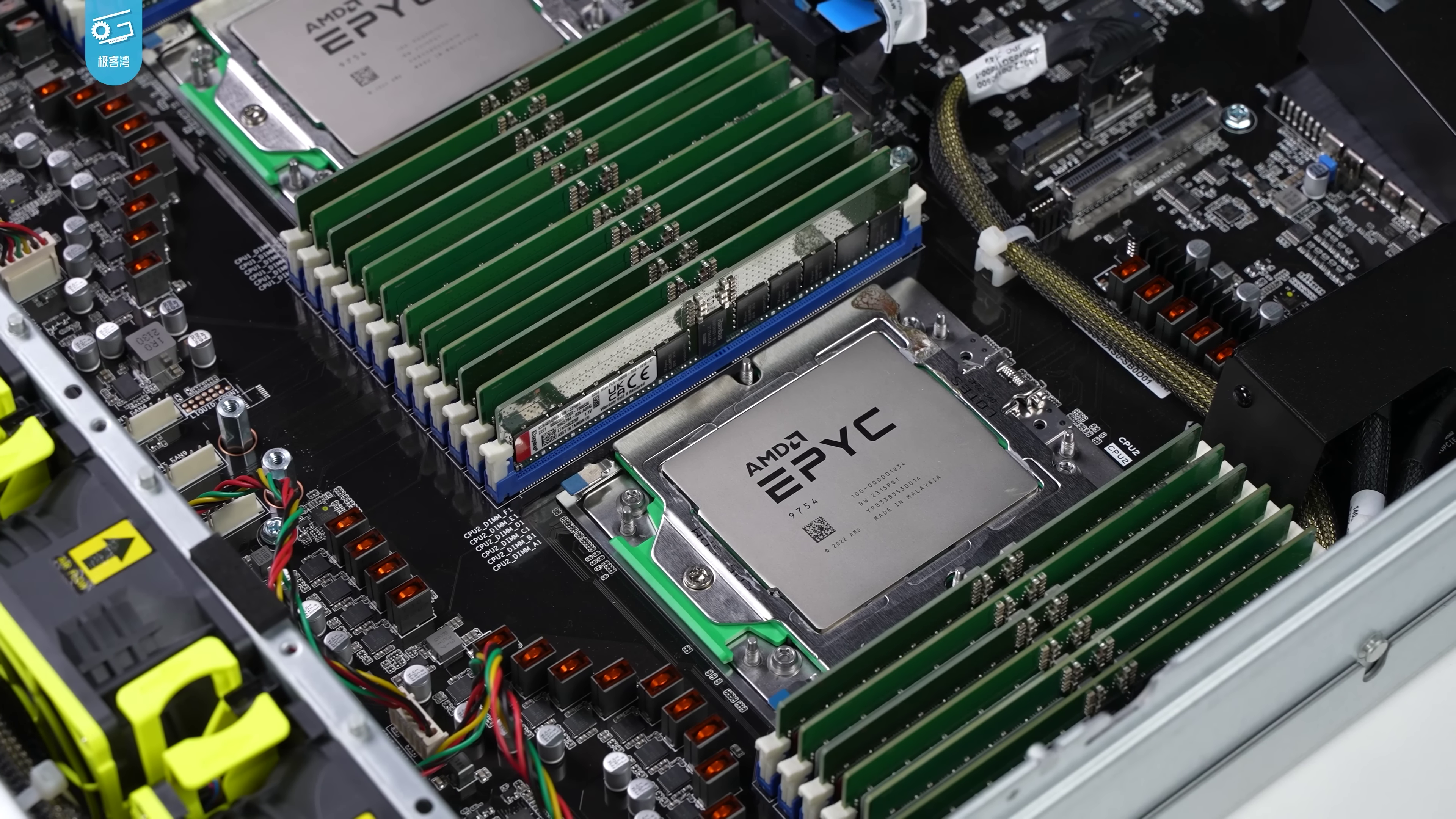
Semiconductor technology has reached a critical milestone with the introduction of IBM’s sub-1 nanometer chip technology. This breakthrough, developed in collaboration with leading semiconductor partners, pushes transistor density to unprecedented levels—nearly twice that of IBM’s previous 2 nm node—while maintaining performance and efficiency gains.
The new architecture, called 'nanostack,' stacks transistors vertically rather than arranging them side by side on a flat plane. This three-dimensional design allows for finer scaling, with dimensions approaching atomic levels at 0.7 nm (7 angstroms). The result is a chip that can deliver up to 50% more performance or 70% greater energy efficiency compared to current 2 nm chips.
This innovation extends beyond transistor density. By enabling different material combinations in each stacked layer, the nanostack architecture optimizes individual transistor performance without compromising overall power efficiency. This flexibility is crucial for advanced workloads like generative AI and high-bandwidth data processing, where both speed and energy consumption are critical.
While IBM has historically led semiconductor advancements—from early transistors in the 1960s to the first 2 nm chip—the sub-1 nm technology represents a shift from traditional scaling. Transistor nodes now refer more to manufacturing generations than exact physical dimensions, but IBM’s 7 angstrom node demonstrates that continued progress is possible even at these extreme scales.
The development was validated through experimental processes including ultra-thin dielectric bonding and dual-channel engineering, confirming the technology’s viability for real-world computation. Additional research presented at VLSI 2026 shows a 40% scaling improvement in SRAM, which could significantly enhance chip efficiency while meeting the demands of next-generation AI systems.
IBM’s semiconductor roadmap projects that this breakthrough will support at least another decade of scaling advancements. The company is also expanding its leadership in quantum computing with plans to launch Anderon, a pure-play quantum foundry, further solidifying its position in advanced manufacturing.
The partnership behind this technology includes industry leaders like Lam Research, Tokyo Electron, and SCREEN Semiconductor Solutions, all working together at IBM’s Albany research facility. This site will soon house a High Numerical Aperture Extreme Ultraviolet (High NA EUV) lithography tool from ASML, essential for producing smaller, more powerful chips.
While the sub-1 nm technology is expected to reach production within the next five years, its long-term impact remains to be seen. The ability to scale below 1 nm could redefine computing capabilities, but challenges in manufacturing precision and material stability will need to be addressed before widespread adoption.