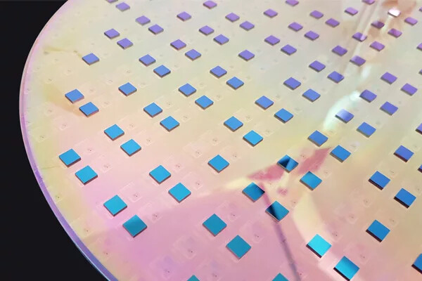
For the first time, researchers have demonstrated functional test structures using die-to-wafer (D2W) hybrid bonding at a 1-micron pitch—a critical step toward building ultra-high-density interconnects for AI hardware.
The breakthrough, presented at a recent industry conference, addresses one of the most pressing constraints in semiconductor design: how to stack multiple dies while maintaining signal integrity and bandwidth. As traditional scaling hits physical limits, this technology offers a path forward by stacking device layers with unprecedented precision.
At a glance
- Pitch: 1-micron interconnects (world-first for D2W bonding)
- Key challenge: Alignment accuracy at this scale remains a hurdle
- Next target: 0.5-micron pitch expected in future iterations
- Applications: AI accelerators, smart vision systems, and multi-die stacking architectures
The technique combines fine-pitch copper-to-copper bonding with inter-die gap filling (IDGF) and through-silicon vias (TSVs), enabling vertical interconnects that could significantly reduce power consumption while boosting performance. Current electrical testing confirms expected yields for pitches down to 2 microns, though 1-micron production is still limited by tooling constraints.
Why it matters
This isn't just another incremental improvement—it's a foundational shift in how chips are built. The ability to stack dies with such precision could redefine the architecture of AI accelerators, where bandwidth and power efficiency are critical. However, real-world adoption depends on overcoming alignment challenges and refining the planarization process for mass production.
What’s next
The roadmap includes a second-generation test vehicle targeting 0.5-micron pitch, with a focus on integrating this technology into multi-die stacking solutions. If successful, it could pave the way for more compact, high-performance systems—though whether it will be ready in time to meet the demands of next-gen AI remains an open question.