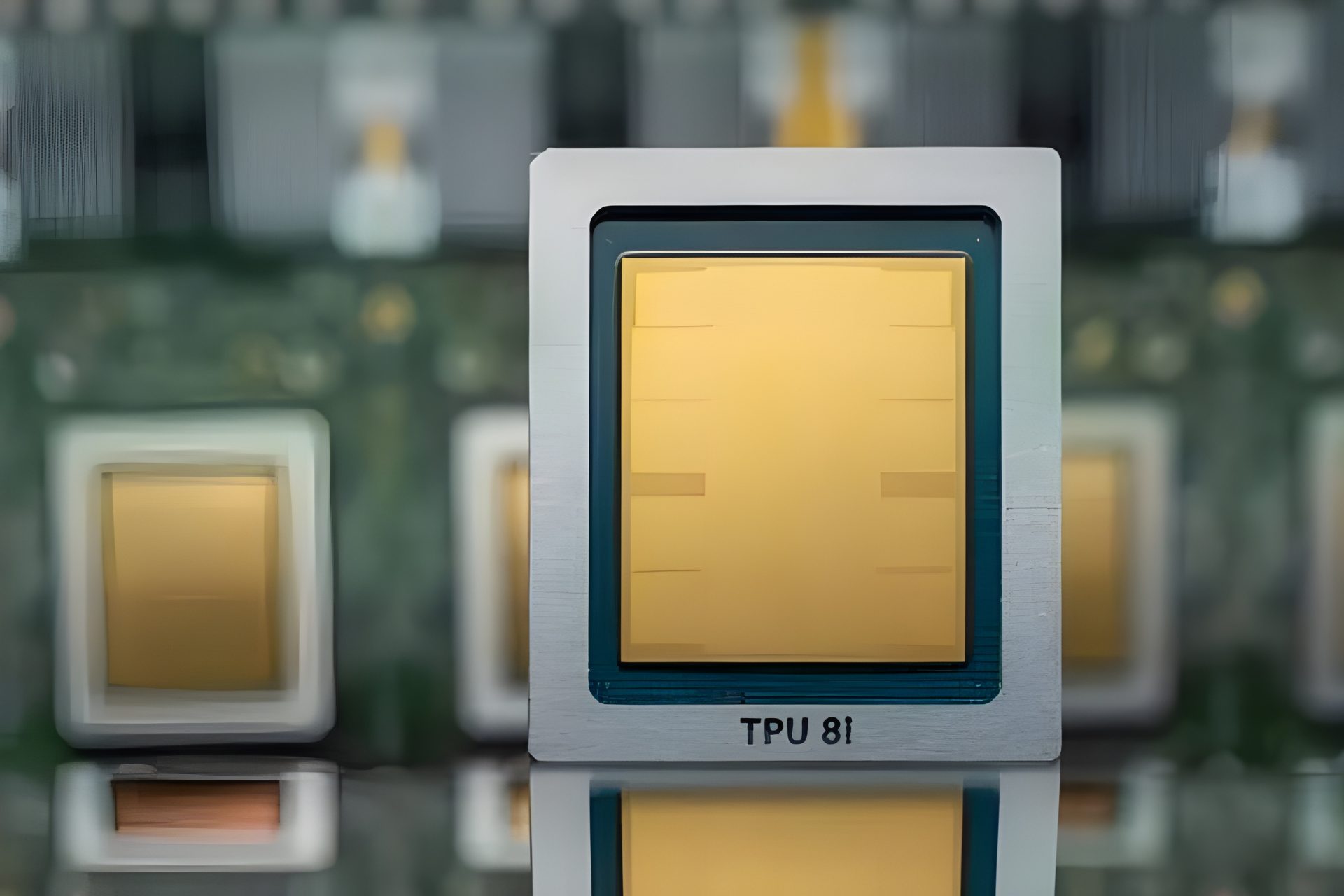
Marvell Scores Another Win After NVIDIA CEO’s Trillion-Dollar Praise, As Google Hands It A Custom Networking Chip For The TPUv8e On Intel’s 18A/18AP Process Rohail Saleem • at EDT Add on Google An efficient networking chip appears to be the need of the hour as AI data centers rapidly fill up with a giga-ton of ASICs, GPUs, and orchestration-oriented CPUs. As such, it is hardly a surprise that Google now appears to have tapped Marvell to design a custom networking chip for its TPUs on one of Intel's advanced node processes. Google is tackling the data latency conundrum head-on by tapping Marvell to design a custom networking chip for its TPUs on Intel's advanced lithography For the benefit of those who might not be aware, a networking chip links individual ASICs to form a synchronized data-crunching behemoth. These chips primarily coordinate the flow of data between ASIC clusters, managing data congestion, operational synchronization, and data latency in real time. Related Story MediaTek Says Its Next-Gen Program Will Only Use Intel’s EMIB-T For Packaging Funda AI: "Marvell will design a networking chip for Google. This chip will be manufactured on Intel's 18A (or 18AP), with mass production scheduled to begin by the end of 2027, and it will be paired with the MediaTek-designed Humufish for Google."$INTC— Jukan @COMPUTEX (@jukan05) June 3, 2026 Now, according to Funda AI and cited by the tipster Jukan, Google has apparently tasked Marvell with designing a custom networking chip for its TPUs. Critically, given the current bottleneck at TSMC when it comes to its advanced nodes, the proposed networking chip is likely to leverage Intel's advanced lithography process, either the 18A or the 18AP. What's more, the networking chip is expected to enter volume production by the end of 2027, which means it will likely be paired with the upcoming Humufish TPU (TPUv8e), where Google is currently designing the ASIC's main die, with MediaTek relegated to the I/O and back-end design, and Intel handling chip fabrication and EMIB-based packaging. Do note that Google has already deployed its TPUs across at least 11 distinct data center regions across the globe, including 2 dedicated "AI zones," which speaks volumes as to the necessity of an efficient networking chip to harmonize the operational cadence of these data centers. Of course, this development marks another win for Marvell, which is currently riding the proverbial high horse in the wake of an emphatic endorsement from NVIDIA's CEO, who now believes it is "the next trillion-dollar company." About the : Writing is my one incontrovertible passion. Over the past six years, he has authored over 2,200 distinct articles on financial and tech-related topics, spanning nearly 1 million words. And he has been a member of Wcctech mobile team since 2025. As an alumnus of the University of Toronto, Rotman Commerce Program, I bring nuance, in-depth knowledge, and a unique perspective to every topic that I cover. When I'm not writing, I'm traveling the world, exploring hidden confectionaries and restaurants as an aspiring food connoisseur. Follow on Google to get more of our news coverage in your feeds. Further Reading Intel’s EMIB-T Packaging Pulls Two More Taiwanese Suppliers Into Google’s TPU Orbit as TSMC’s CoWoS Strains Intel’s 288-Core Clearwater Forest Xeon 6+ Lands on 18A, Claiming 30% Performance & 50% Efficiency Lead Over AMD’s 192-Core EPYC Intel Intros Diamond Rapids “Xeon 7” CPUs Built On 18A-P: Packing Up To 192 Cores, 16-Channel Memory, PCIe Gen6 Support, Launching In 2027 A Scuba Diver Just Pulled An Unreleased Google Pixel Watch 5 From The Caribbean Seabed After A Google Employee Dropped It Read all on Marvell Scores Another Win After NVIDIA CEO’s Trillion-Dollar Praise, As Google Hands It A Custom Networking Chip For The TPUv8e On Intel’s 18A/18AP Process