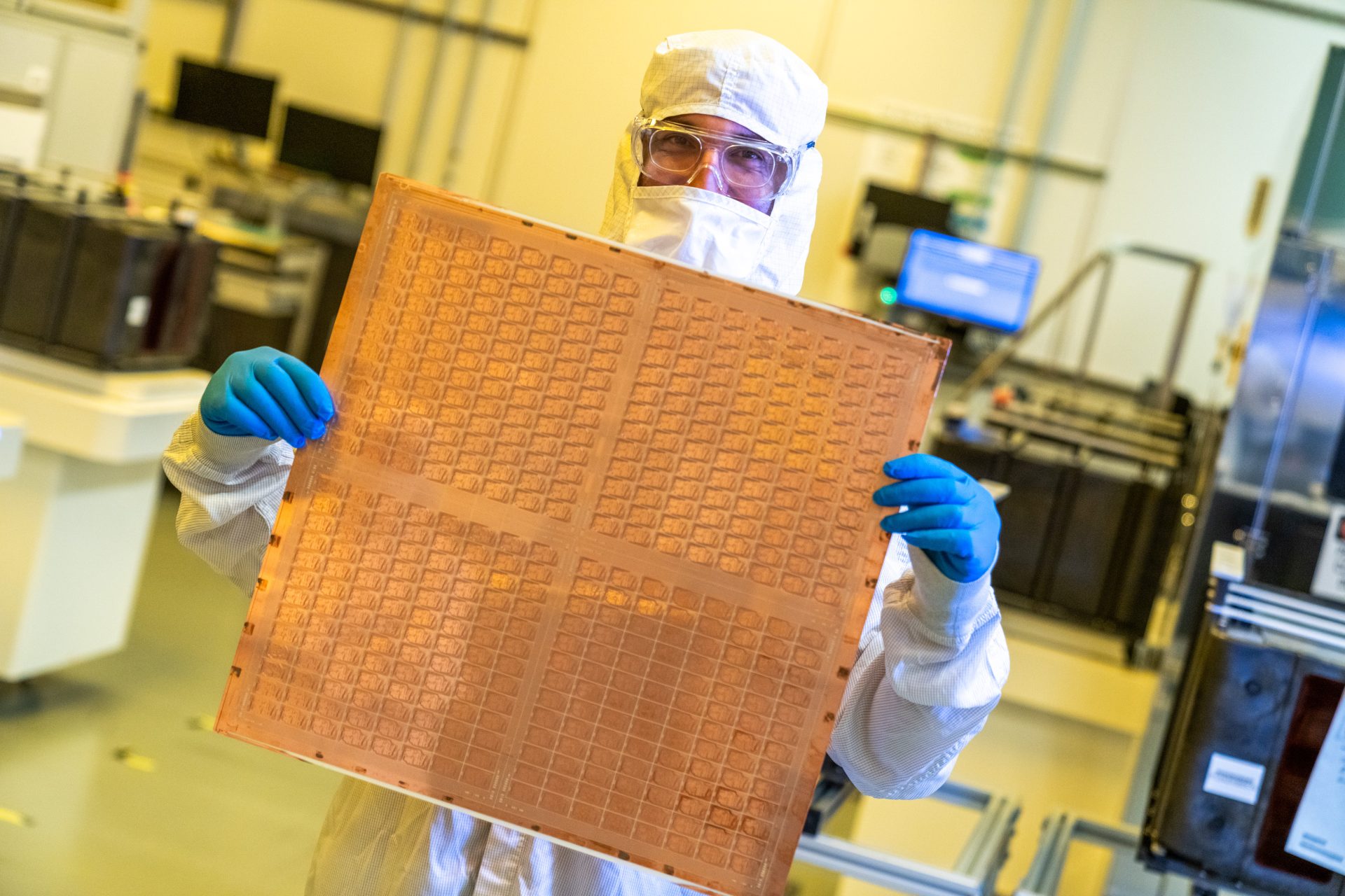
A new era in semiconductor packaging is emerging, one that could fundamentally alter the landscape of device manufacturing. The development of glass substrate technology, spearheaded by a major player in the industry, is poised to deliver substantial improvements in performance and efficiency. This shift is not just about incremental gains; it's about redefining what's possible in the field.
The focus here is on glass substrates, which offer a more robust and efficient platform for semiconductor packaging compared to traditional methods. This technology leverages the unique properties of glass—its thermal stability, electrical insulation, and mechanical strength—to create a more reliable and high-performance foundation for chips. The potential impact extends beyond just performance metrics; it could also streamline manufacturing processes, reducing costs and improving yields.
What sets this advancement apart is its commercial readiness timeline. Industry insiders suggest that within three years, this technology will be fully operational in production lines, marking a significant milestone in the semiconductor industry's evolution. This is not merely an incremental step; it represents a paradigm shift that could set new benchmarks for efficiency and performance.
The implications of this development are far-reaching. For one, it addresses the growing demands for higher performance and more compact designs in modern electronics. As devices become more complex and power-hungry, traditional packaging methods struggle to keep up. Glass substrates, with their superior thermal properties, could provide a solution that meets these challenges head-on.
Additionally, this technology could pave the way for more advanced cooling solutions, which are crucial as chip densities continue to increase. Efficient heat dissipation is a critical factor in maintaining performance and longevity in electronic devices. By integrating glass substrates into the manufacturing process, industry leaders aim to tackle these challenges effectively, ensuring that future generations of chips can operate at optimal levels without compromising on reliability.
Looking ahead, the adoption of glass substrate technology could also open doors for innovations in areas like 3D packaging and heterogeneous integration. These advancements are essential as the industry moves towards more sophisticated and multi-functional devices. The ability to stack multiple layers of chips with precision and efficiency will be key to unlocking the full potential of next-generation electronics.
For now, the focus remains on refining the technology and preparing for its commercial rollout. While there's still work to be done, the progress so far is promising. Industry experts are optimistic that this development will not only meet but exceed expectations, setting a new standard for semiconductor packaging.