Semiconductor innovation often hinges on pushing physical limits, and a recent breakthrough in 2D material transistors offers a glimpse into what’s next for chipmaking. The challenge has long been balancing performance with scalability—achieving smaller, faster transistors without sacrificing reliability or manufacturability. Now, ASML, TSMC, and imec have demonstrated a scalable 300 mm integration process for 2D-material-based nFETs and pFETs, achieving a contacted poly pitch of just 50 nm—a critical metric for advanced logic nodes.
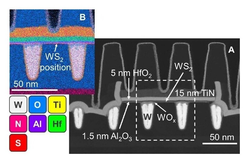
This achievement marks the first time such transistors have been produced at industry-relevant dimensions while maintaining performance comparable to lab-scale devices. The collaboration leverages extreme ultraviolet (EUV) lithography, a technology already proven in high-volume manufacturing, to pattern transistors with channel lengths as small as 28 nm. That sharpness was key to overcoming one of the biggest hurdles: contact resistance. Traditional 2D-material transistors often require larger contacts to maintain performance, limiting further scaling. By optimizing the integration flow—using bottom contacts and an overlapping gate—the team eliminated that bottleneck.
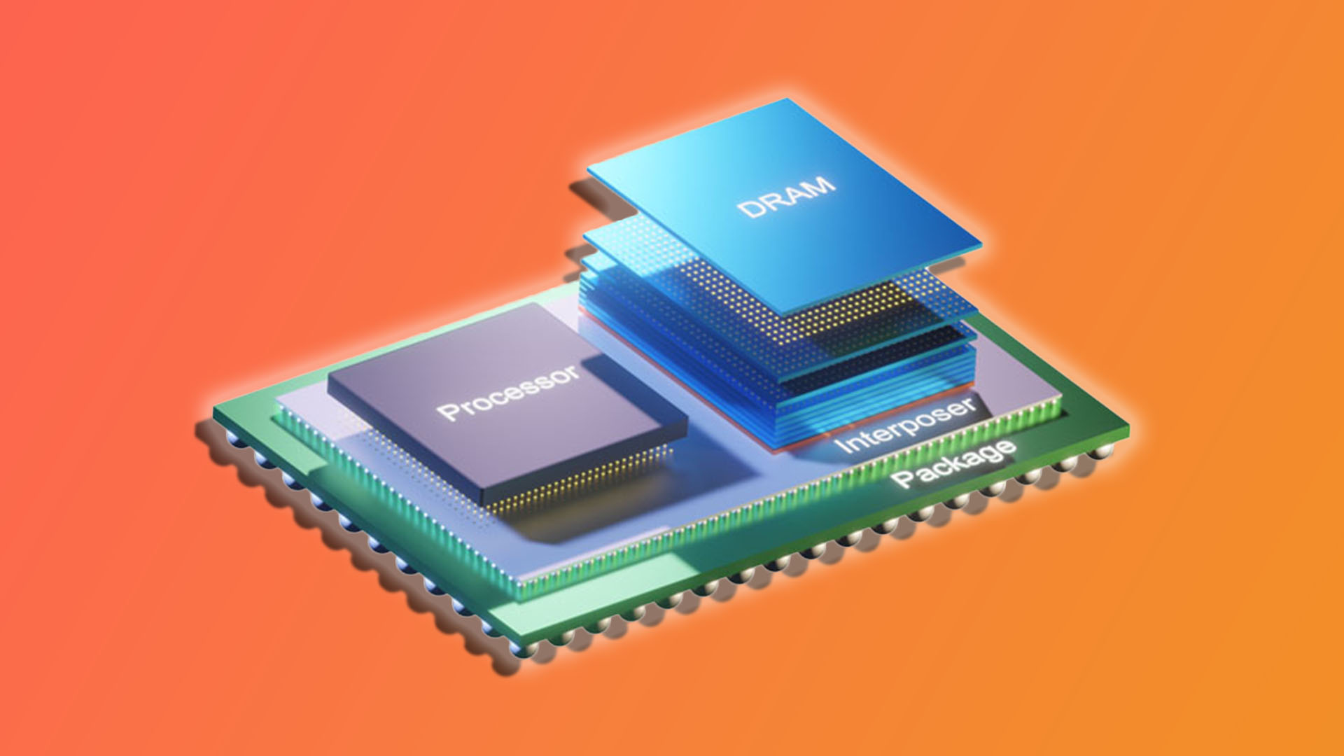
The results are promising: both nFETs (with MoS₂ channels) and pFETs (WS₂ or WSe₂-based) show excellent current-voltage characteristics, with off-currents near zero at zero gate voltage. Operational yields are high, with 94% of transistors meeting performance thresholds, suggesting the process is robust enough for real-world fabrication. The approach isn’t limited to MoS₂, WS₂, or WSe₂; it’s designed to work with other 2D-channel materials, opening doors for future experimentation.
What This Means for Chipmakers
- Performance at Scale: 2D-material transistors could outperform silicon in ultra-scaled nodes, but only if they can be mass-produced. This work proves that’s possible with today’s lithography tools.
- Back-End Applications: Beyond logic chips, these materials show potential for back-end-of-line and wafer backside applications, where their electrostatic properties could enable new architectures.
- EUV’s Role: The use of EUV lithography—already deployed in 3 nm and 2 nm nodes—means this isn’t a distant future technology. It’s being tested today with proven equipment.
The collaboration underscores the importance of partnerships in de-risking emerging technologies. TSMC, for instance, has emphasized that such research is about accelerating discoveries from labs to factories—a critical step as the industry races toward sub-3 nm nodes. ASML’s involvement highlights how EUV lithography isn’t just a tool for today but a foundation for tomorrow’s breakthroughs.
Yet challenges remain. While the 50 nm pitch is a milestone, real-world adoption will depend on further scaling, cost reductions, and compatibility with existing manufacturing lines. The team acknowledges that this is an early step, but the direction is clear: 2D materials are no longer a theoretical possibility; they’re becoming a practical path forward.
For buyers and investors, the takeaway is simple: keep an eye on how quickly this technology transitions from research to production. If it follows the trajectory of EUV lithography—adopted faster than many expected—the next generation of chips could arrive sooner than anticipated.