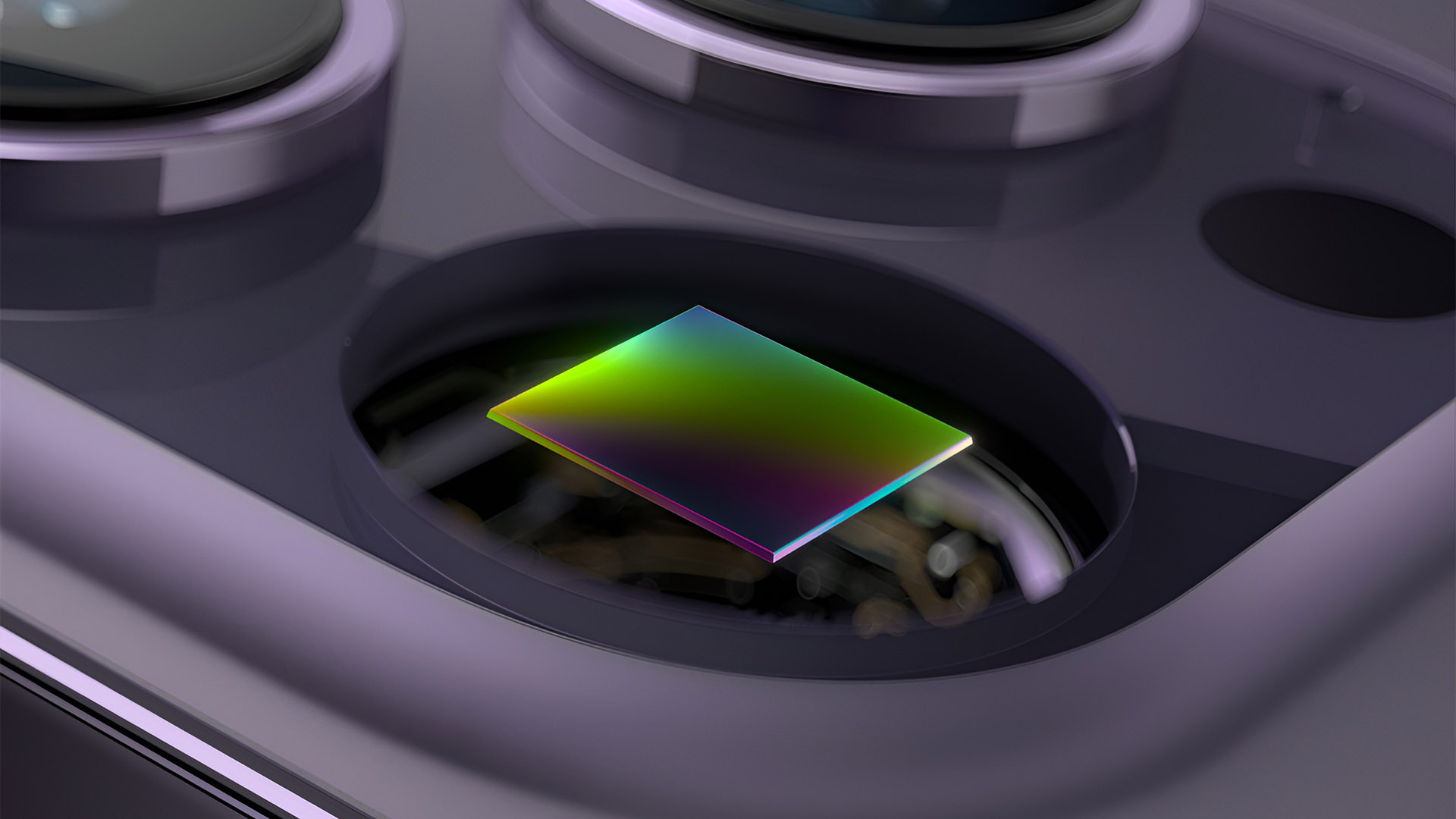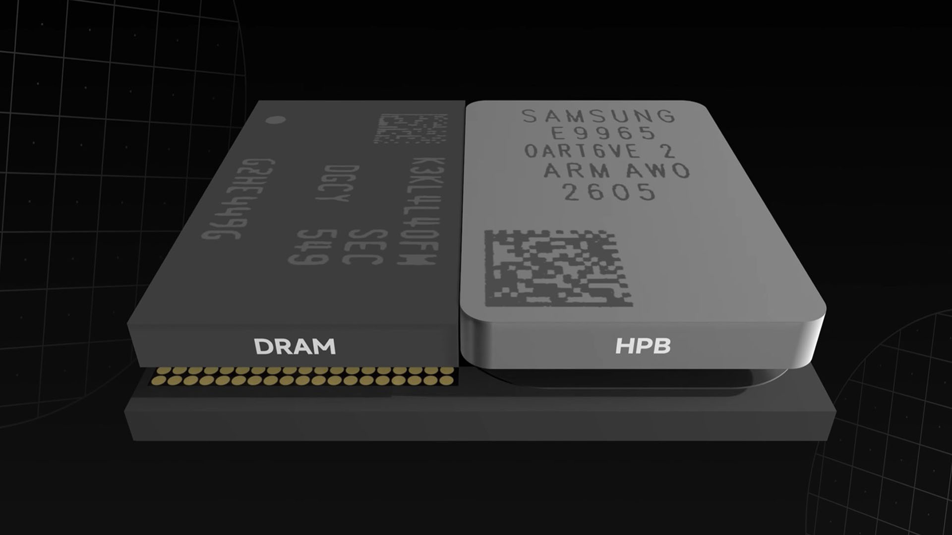
The Exynos 2600 SoC marks a paradigm shift in mobile processing, addressing long-standing limitations in performance density and thermal efficiency. By transitioning to Samsung's proprietary 2 nm GAAFET process—equivalent in performance to TSMC's N2 node—the chip achieves a balance between raw power and energy consumption that previous generations struggled to match. This advancement is not just incremental; it represents a fundamental rethinking of how mobile devices can handle complex workloads while maintaining battery life and thermal control.
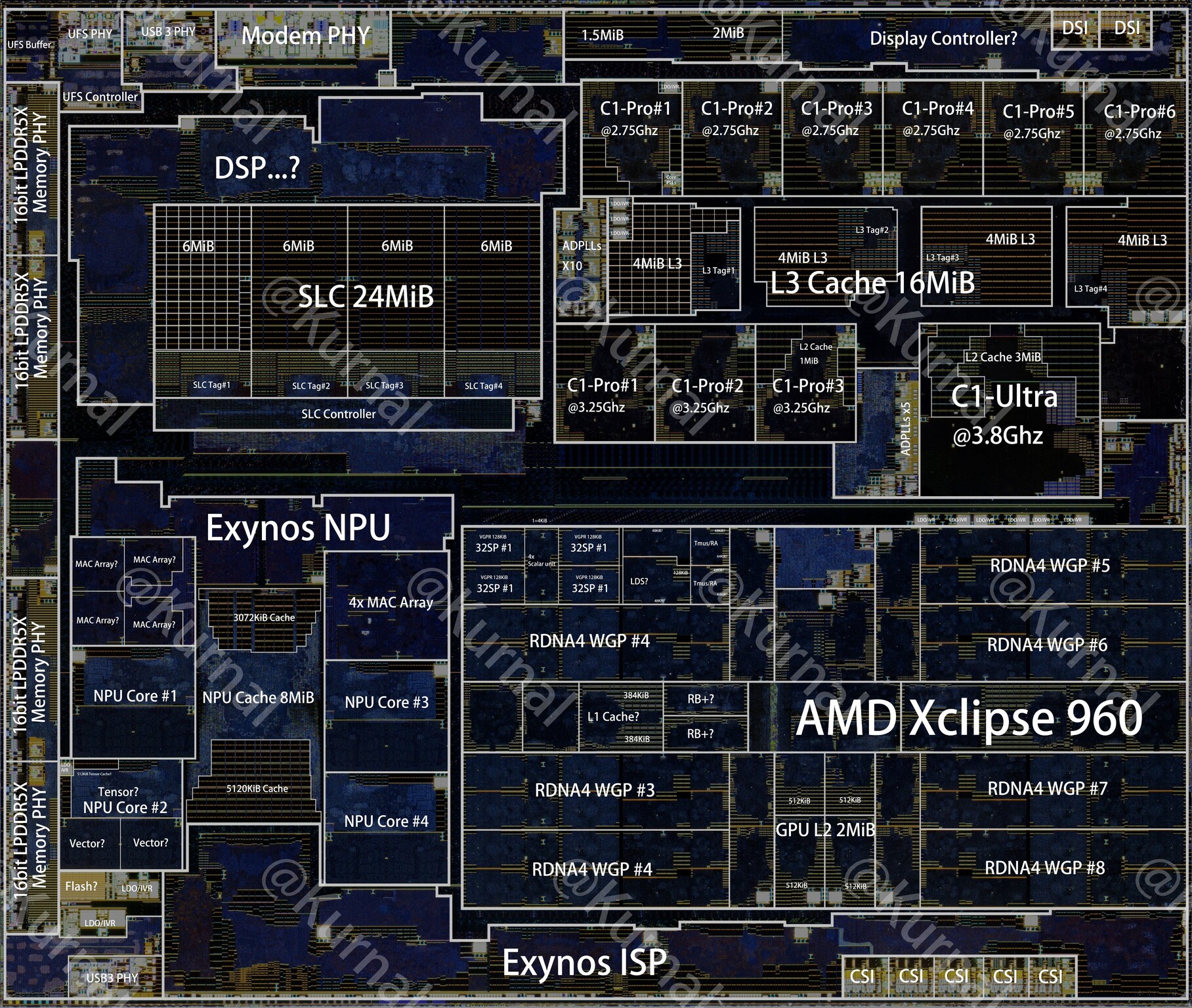
At the core of this transformation is a sophisticated three-tiered CPU architecture, designed to optimize performance across different types of tasks. The ultra-core, clocked at up to 3.80 GHz, features 3 MB of dedicated L2 cache, ensuring it can tackle the most demanding computational challenges with minimal latency. Complementing this are three performance cores, each running at up to 3.25 GHz and equipped with 1 MB of L2 cache, while six efficiency cores, capped at 2.75 GHz, handle lighter workloads. All ten cores share a substantial 16 MB L3 cache, which acts as a buffer for seamless coordination between different processing tasks, reducing bottlenecks in multitasking scenarios.
The GPU within the Exynos 2600 is another area where significant strides have been made. Leveraging AMD's RDNA 4 architecture through the Xclipse 960 iGPU, this component introduces 16 compute units spread across eight workgroup processors, totaling 1,024 stream processors. Paired with 64 TMUs and 32 ROPs, along with 4 MB of dedicated L2 cache, the GPU is optimized for graphics-intensive tasks such as gaming and multimedia consumption on mobile devices. This level of graphical fidelity was previously reserved for high-end desktop GPUs, but its integration into a mobile SoC represents a major leap forward in on-device rendering capabilities.
For AI workloads, the Exynos 2600's NPU delivers over 100% performance improvement compared to its predecessor. With a 32K MAC design spread across six cores—each featuring four MAC arrays and dedicated Tensor/vector hardware—the NPU achieves a real-world throughput of 59 TOPS. This is further supported by an 8 MB scratchpad RAM, which ensures efficient handling of complex AI tasks such as real-time image processing, natural language understanding, and on-device machine learning. The NPU's performance is particularly noteworthy given the increasing demand for AI capabilities in mobile devices, from advanced camera features to personalized assistant interactions.
Why It Matters for Upgrades
The Exynos 2600's advancements are not just about raw numbers; they address practical challenges that have hindered the progression of mobile computing. The transition to a 2 nm GAAFET process allows for more compact and energy-efficient designs, which could lead to thinner, lighter devices without sacrificing performance. This is a critical factor for manufacturers looking to push the boundaries of what mobile platforms can achieve while maintaining thermal control—a long-standing bottleneck in high-performance mobile SoCs.
For IT teams evaluating upgrades, the Exynos 2600 offers a compelling mix of performance and efficiency that could serve as a catalyst for adopting new architectures. The three-tiered CPU design ensures that power is managed more effectively, which is crucial for maintaining battery life—a key concern for mobile platforms. Additionally, the RDNA 4-based GPU and the high-performance NPU provide capabilities that were previously only available in more expensive or larger devices, making them accessible to a broader range of products.
Who Benefits?
Enthusiasts and power users stand to gain the most from the Exynos 2600's enhanced features. The RDNA 4-based GPU promises smoother graphics performance, which is ideal for gaming and multimedia applications on mobile devices. This could redefine the user experience for those who rely on their smartphones or tablets for intensive graphical tasks, providing a level of fidelity that was previously unattainable in portable form factors.
Meanwhile, the NPU's significant AI performance boost could revolutionize how smartphones handle tasks like real-time image processing and on-device machine learning. This is particularly relevant as AI becomes more integrated into everyday mobile experiences, from advanced camera features to personalized assistant interactions. For everyday users, while the immediate benefits may not be as noticeable, the underlying architecture lays the groundwork for future-proofing devices, ensuring they remain capable of handling emerging demands.
The Exynos 2600's transition to a 2 nm GAAFET process also paves the way for more compact and energy-efficient designs. This could lead to thinner, lighter devices that do not compromise on performance, addressing one of the long-standing challenges in mobile computing. The result is a chip that not only meets but exceeds the expectations set by previous generations, offering a compelling mix of performance, efficiency, and AI capabilities.
In summary, the Samsung Exynos 2600 represents a significant step forward in mobile processing. It offers a blend of advanced CPU architecture, high-performance GPU, and cutting-edge NPU that could redefine what is possible in mobile computing. For manufacturers, this chip presents an opportunity to push the boundaries of device capabilities while maintaining thermal control and battery efficiency. The real question is whether they will fully capitalize on these advancements to deliver devices that meet the evolving demands of both power users and everyday consumers.