NVIDIA’s next major AI accelerator, the ‘Feynman’ GPU set for 2028, will split its manufacturing process between TSMC and Intel Foundry, according to recent industry reports. While the bulk of the chip’s compute cores will still be fabricated at TSMC using its advanced 1.6nm A16 process—accounting for roughly 75% of the chip’s value—the final packaging and chiplet bonding will shift to Intel’s U.S.-based facilities. This hybrid approach reflects NVIDIA’s growing reliance on Intel’s EMIB (Embedded Multi-die Interconnect Bridge) technology for interconnecting components, a departure from its long-standing TSMC-centric strategy.
The decision underscores NVIDIA’s effort to mitigate geopolitical risks tied to semiconductor imports, particularly as U.S. tariffs and export controls tighten. By packaging the ‘Feynman’ GPU in the U.S., the company avoids potential penalties while still accessing TSMC’s leading-edge process nodes for critical performance components. Intel’s 18A and 14A nodes will handle peripheral silicon, though TSMC’s A16 remains the backbone of the design.
A Memory Leap and Trillion-Parameter Models
The ‘Feynman’ GPU is also expected to adopt next-generation memory standards, likely HBM4e or HBM5, to deliver substantially more memory bandwidth per package. This upgrade aligns with NVIDIA’s push into trillion-parameter AI models, where memory capacity and bandwidth are key bottlenecks. Early benchmarks suggest the architecture could support workloads far beyond current offerings, though exact performance figures remain under wraps.
Why the Shift to Intel?
NVIDIA’s move follows its $5 billion investment in Intel late last year, a deal that granted it a 5% stake in the foundry giant. The partnership signals a broader realignment in the semiconductor industry, where companies are increasingly hedging bets against supply chain disruptions. For Intel, the collaboration represents a rare win in its foundry business, which has struggled to compete with TSMC and Samsung in advanced nodes. By handling packaging and chiplet integration, Intel avoids direct competition with TSMC on cutting-edge processes while gaining a foothold in NVIDIA’s high-margin AI market.
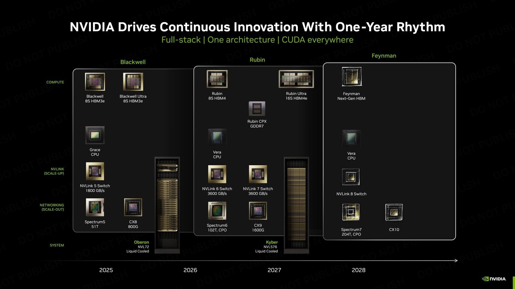
Industry observers note that the ‘Feynman’ GPU’s design may also reflect NVIDIA’s internal debates over long-term manufacturing strategy. While TSMC remains the gold standard for performance, Intel’s EMIB technology offers a compelling alternative for multi-chip modules, particularly as AI workloads demand ever-larger die sizes. The hybrid approach could set a precedent for future GPUs, where packaging becomes as critical as silicon fabrication.
Reaction: A Calculated Gamble
Early industry reaction suggests the announcement is being viewed as a pragmatic step rather than a dramatic shift. Analysts highlight that NVIDIA’s core architecture—including its proprietary Ampere or Blackwell derivatives—will still rely on TSMC for the most advanced nodes, ensuring performance leadership. However, the use of Intel for packaging could accelerate U.S. manufacturing goals, particularly as the Biden administration pushes for domestic semiconductor production.
Some speculate that the ‘Feynman’ GPU’s memory advancements—potentially HBM5—could also pressure AMD and other competitors to accelerate their own high-bandwidth memory roadmaps. With AI training costs soaring, memory efficiency is becoming a differentiator, and NVIDIA’s move may force rivals to rethink their strategies.
What Comes Next?
While the ‘Feynman’ GPU isn’t expected to reach consumers until 2028, its development hints at broader trends in AI hardware. The integration of Intel’s foundry capabilities may signal a more fragmented but resilient supply chain, where companies distribute manufacturing risks across multiple partners. For now, NVIDIA’s focus remains on delivering the next leap in AI performance, with ‘Feynman’ poised to tackle workloads that current GPUs—even the RTX 5090—cannot handle.
The $5,000 RTX 5090, released last year, remains the most powerful consumer GPU on the market, but its architecture is already showing signs of strain under the demands of trillion-parameter models. The ‘Feynman’ GPU’s memory and compute advancements could redefine the landscape, though its exact specifications—and whether it will target data centers or high-end workstations—remain unclear.