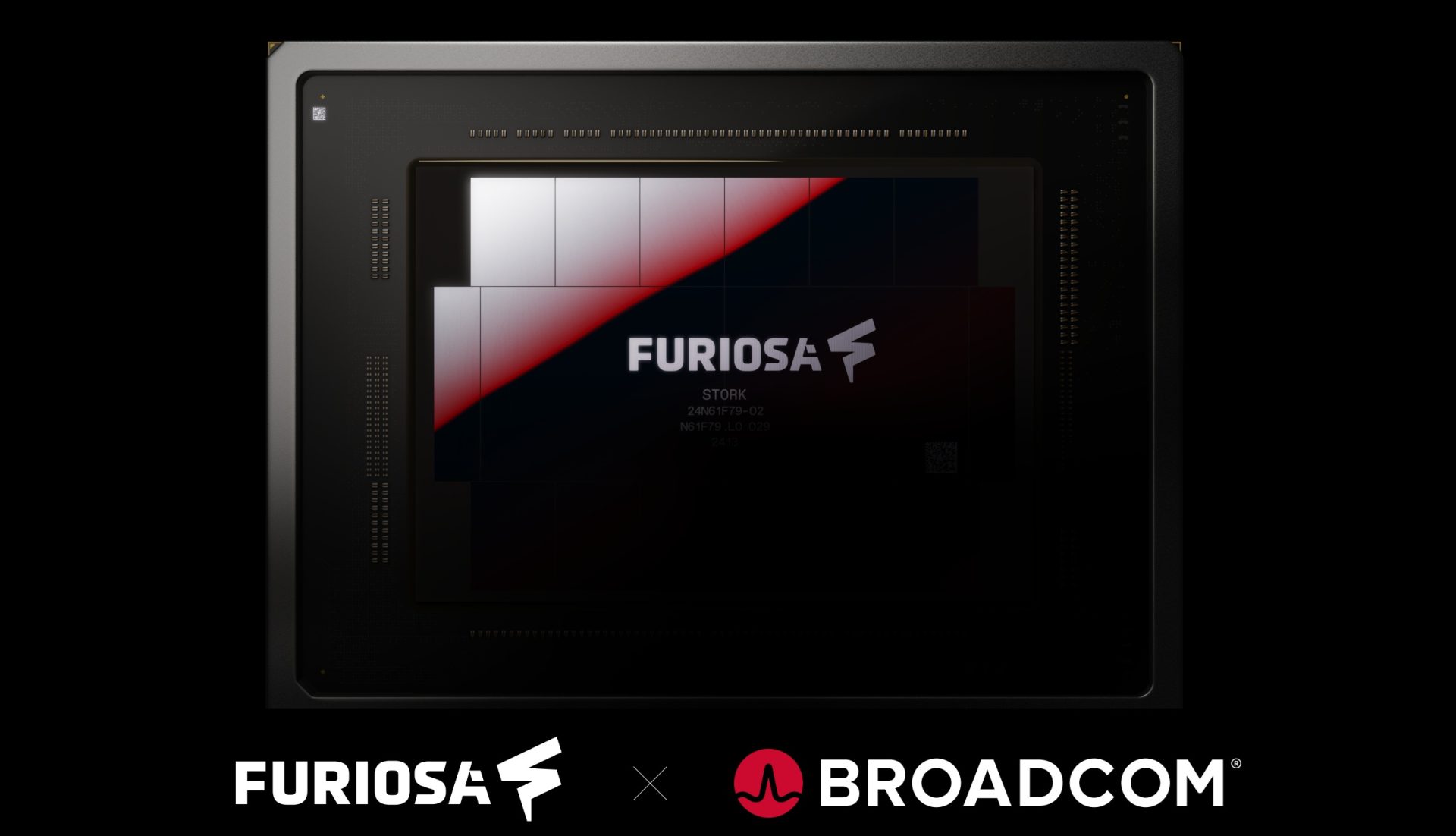
inference hardware has always been a balancing act between performance and power, but FuriosaAI’s latest 2 nm chip shifts that balance dramatically. By integrating multiple HBM4e stacks directly into the package, it achieves memory bandwidth of 1.2 Tbps per stack—far exceeding what GPUs typically manage with their GDDR or HBM interfaces—while maintaining power efficiency that rivals even the most optimized CPUs.
This isn’t just about raw numbers, though. The design eliminates the von Neumann bottleneck by placing compute units right next to memory, reducing data movement and latency. That means less heat, lower cooling requirements, and workloads that can run longer without thermal throttling—a critical advantage for edge devices or high-density data centers where space and power budgets are tight.
Where the efficiency gains matter most
The chip’s target isn’t just benchmarks; it’s real-world impact. For example, in a typical AI inference workload, GPUs often draw 10-20 watts per TOPS (trillions of operations per second), while this processor aims for sub-5 W/TOPS—closer to what you’d expect from a high-end CPU but with the specialized compute units needed for AI. That efficiency doesn’t come at the cost of performance, either. The architecture includes custom cores optimized for both sparse and dense matrix operations, ensuring it can handle everything from lightweight edge models to more complex inference tasks without sacrificing accuracy or speed.
A 2 nm leap forward
The move to a 2 nm process adds another layer of advantage. TSMC’s latest node delivers higher clock speeds with significantly reduced leakage current, allowing the chip to push performance while staying within strict thermal limits. This is particularly important for edge deployments where heat dissipation can be challenging or where battery life is a concern.
Changing the conversation
While GPUs will likely remain dominant in mixed-precision training and other computationally intensive tasks, this chip is designed to redefine the landscape for inference. It’s not about replacing GPUs but offering an alternative for scenarios where power efficiency is non-negotiable. The result? Fewer cooling systems, lower operational costs, and hardware that can run continuously without trade-offs in performance.
- Process: 2 nm (TSMC)
- Memory bandwidth: HBM4e, 1.2 Tbps per stack
- Compute units: Custom inference cores for sparse/dense matrices
- Power efficiency: Sub-5 W/TOPS target
- Package: Advanced 3D stacking with multiple HBM4e stacks
The focus isn’t just on the hardware itself but on the broader implications. If this chip gains traction, it could shift the way IT teams think about AI deployments—moving away from brute-force performance and toward solutions that deliver the same (or better) results with far less power. That’s a paradigm shift worth watching.